If you’ve ever designed a PCB, it being purely electronic, electromechanical or electrochemical you know during engineering you’re bound by manufacturing constrains. If your problem-solving-product passed all the DFX tests and made it to mass production, you’ve had to pick a contract manufacturer (C.E.M) to help you deliver to your customers. Now you’re ready to recharge and embark the next project.
That would be a great story where everyone lives happily ever after. However you figured out soon after the first batch got delivered, yield isn’t something you should be taking for granted. Especially, if you’ve decided to support our UK CEMs, who in some cases, lack behind far eastern counterparts.
As a quick reminder the following equations explain how yield is calculated
Let:
P = Number of units to be produced
G = Percentage(%) of working units ready to be sold
R = Percentage(%) of units needing rework
So if P = 100, G = 0.86 (86%) , R = 0.14 (14%)
The Y(ield) = P*G + P*(1-G)*R = 87.96 meaning next time, you need to produce 12.31 more units to have 100 ready to be sold. The burden arising from imperfect yields can be steep. But…
Why?
While it’s easy for the buisness to put on the designer, or the designer to put it on the CEM, the truth hides somewhere in the fog of war.
As a designer who finished the internal DFX procedures, the next step is to check with your CEM the following bare minimums:
- The PCB Stackup (εr, Df, Td)
- Trace Widths for specific Ζ (impedance)
- Copper-to-copper clearances
- Silkscreen (if there is one)
- VIA Aspect Ratios, VIA filling (if necessary)
- BoMs
- Footprints
Your CEM’s work however doesn’t finish with this tiny checklist. If it does, you’ll get lower yield than you expect.
The CEM is expected to check all the data you’ve provided such as:
- The Profile of the board
- The Silkscreen (and notify you if printing issues)
- The Solder Mask Colour, Openings, Slivers (and notify you of adjustments)
- Each and every copper layer, copper weight (and warn you about copper imbalances to prevent wrapping over time, clearances, necessary adjustments)
- The Solder Paste layer (and execute necessary adjustments)
- The Drill Files (and notify you of issues with unsupported holes, AR, fillings)
- The Drill Map and Drill Chart (when provided)
Failures on the CEM side to examine the data thoroughly, and lack of QC can make you think…
HUH?
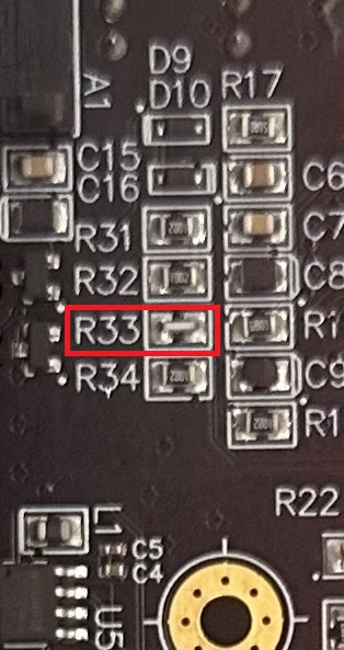
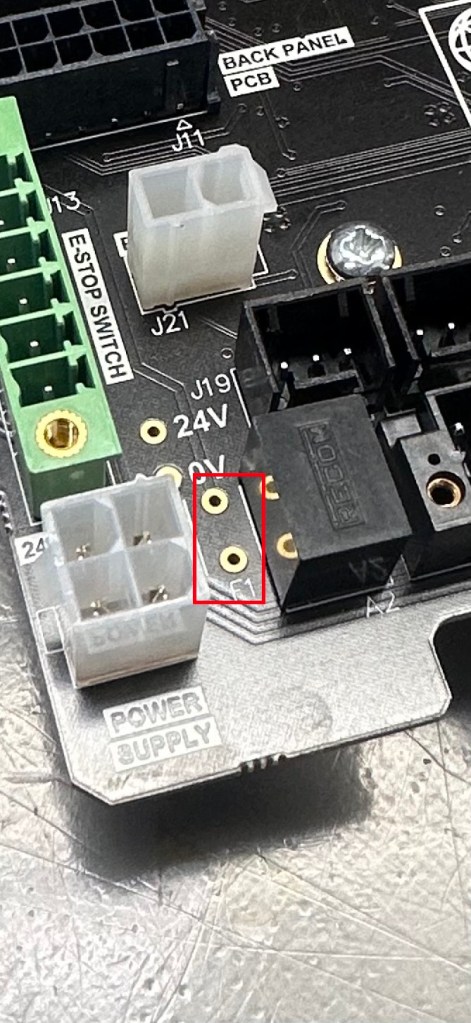
They soldered only one pin of a through hole crystal and insufficiently wetted the other? Ok, it only happend twice.
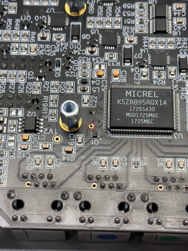
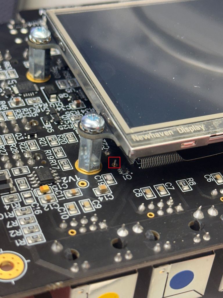
They insufficiently wetted SMD components? Well, again, that only happened twice
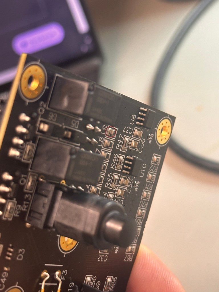
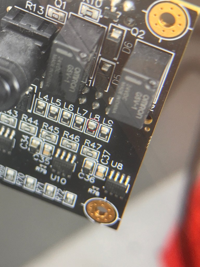
They billboarded a component? They overheated DCDC regulators to the point of melt? They forgot to place through hole fuses on boards? They fitted the wrong part?
That only happened once,twice,thrice etc etc.
So what’s the remedy? There’s never a direct or easy fix, but a combination of actions can improve your yield significantly.
- Test Jigs
- Automated Optical Inspections (These don’t happen ‘by default’ with every supplier)
- JTAG Boundary Scans
- Different assembly techniques (Automated, rather than having a Human-in-the-loop)
The story will be continued on the next post


Leave a comment